Saturday, May 19, 2012

FreeMat Activity in Complex Calculation

Purpose
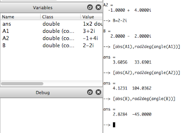
  The purpose of this assignment is to know how to do complex calculation by hand and compared the results to FreeMat.

Assignment


Assignment 1 answer
By Hand
By FreeMat

Assignment 2 answer

Assignment 3 answer
By Hand

By FreeMat

Assignment 4 answer


Impedance and AC Analysis I

Purpose
    This lab has been broken into two parts. The purpose of the first part is to investigate a real-world inductor which is equivalent to connect with RL and L in series, so the impedance ZL can be determined as ZL = RL + jwl and determine the inductance by looking for the ratio of magnitude of the terminal voltage and current phasors by following circuit.
Figure 1. Designed Circuit to Determine L in Part 1.

For second part of this lab, we want to find out at which frequency will the impedance become pure resistive by connecting to the circuit with a capacitor, in other words, the current is at maximin value, and we use that to know how a capacitor will affect the current and impedance of the circuit by adjusting the frequency of function generator in a series RLC circuit. 
Figure 2. Designed Circuit to Determine C to Obtain Pure Resistive Impedance in Part 2.

Assemble
Figure 3. Build-up Circuit

Figure 4. Build-up Series RLC circuit connected to FG, O-scope, and Multimeters.

Approach
    First, we set up the frequency and RMS value of function generator to 20.0kHz and 5.00 V and the output signal is sinusoid. After we build the circuit as showing above , the Vin,rms and Iin,rms reading are 4.52 V and 88.0mA. The reason why the reading differ from the FG display is due to the FG's internal     
resistance. So, the total impedance of the circuit is 4.52/88mA which equals to 51.36 ohms. Since we know that Z can be written as Z=(Rext+RL)+jwl, and its magnitude is square root[(Rext+RL)^2-(wL)^2]. The angular can be calculated as w=2pi*f = 2 *pi *20k = 125664 rad/s. By substitute all data into square root[(Rext+RL)^2-(wL)^2] = abs(Z), we can get the impedance is 0.4 mH.
Next, we want to figure out at what C value  can cancel the imaginary part of the impedance due to L from previous part of lab. We simply set up XL=XC, and then we can get XC is equal to 50.27. Since XC = 1/wC ==> C= 1/(2*pi*20k*50.27) = 1.58*10^-7 F. However, we get only reach 0.151 uF of capacitance, so we redo the math to calculate the frequency that will cancel the imaginary part of the impedance which is our goal. f = 1/(2*pi*50.27*.151u) = 20.97 kHz.

Data
We take scope measurement at 20.97 kHz.
Vp-p,ch1 = 23.08 V
Vp-p,ch2 = 19.49 V
delta t = 19.46 us
The phase difference = delta t * f *360 degree = 19.46 u* 20.97k * 360 degree = 146 degrees
Recorded the DMM measurements by adjusting the frequency of FG

Table 1. Recorded data of voltage, current and computed Z in Part 2.
Follow-Up Questions
  • Why is the input current the largest at 20.97 kHz?

At 20.97 kHz, the imaginary part of Z will be cancel, so Z value is at the minimum. Also, by Ohm's Law, I = V/Z. When Z is minimum, I will be maximum.

  • Calculate the theoretical voltage phasor across the real inductor at 20.97 kHz. Compare this with the scope measurements by converting those into RMS. 

Theoretical Value (volts):

Experimental Value (volts):
% error:
  • The circuit looks more capacitive at frequencies below 20.97 kHz; the circuit looks more inductive at frequencies above 20.97 kHz.




AC Signal #1

Purpose
    The purpose of this lab is to explore the phase difference between AC sine signals at the same frequency in a simple RC circuit; besides, by adjust the frequency of the signal and resistance in the circuit, the phases will be different. Also, we can learn how to read the value of current or voltage on the scope display.


Knowledge
    If we can find that the amplitude of voltage is 6 divisions in 2V/Div scale from the scope, we can know the reading of voltage is 12V. Assumed that 6 divisions of horizontal time base set to 10 us/div, and we can find the period is 60 micro sec, and frequency is 1/T.  Between two peaks of two different channel of the signals, the phase difference between them would be t*f*360 degrees. If one peak of Ch1 is before Ch2, we call Ch1 signal is leading Ch2 signal.

Circuit
Figure 1. The Desired Circuit
Figure 2. Build-up Circuit connected to O-scope and Multimeter

Set-up
    First, We want to know the phase difference between CH1 and CH2, so we set the FG to produce 1 V peak-peak sine wave at 1k Hz. The RMS value for DMM is 0.318 V. The complex impedance of the 100 nF capacitor can be calculated as 1/(2*pi*C) = 1592 ohms. Next, we connect CH1 to FG and CH2 to the top of capacitor, and then Resistor box and C connected as shown above. After we assemble our circuit, we start measure our data.

Results
Part A
  • peak-peak of CH2 = 0.852 V
  • Vrms CH2 = 0.23 V
  • tx =105.41 micro sec.
  • Phi = tx * f * 360 = 37.9 degrees
==>CH1 is leading CH2 by 37.9 degrees

Part B
Next we adjust the frequency of input signal to 10 kHz rather than 1k Hz. 
  • V peak-peak CH2=0.154V
  • Vrms = 0.033 V
  • tx=23.78 micro sec
  • Phi = tx * f * 360 = 85.6 degrees
Part C
In order to see the impact of resistance, we adjust the resistor box to 10 Kohms, and we take the measurements.
  • V peak-peak CH2 = 0.178 V
  • Vrms = 0.049 V
  • tx = 221.62 micro sec
  • Phi = tx * f * 360 = 79.8 degrees
Figure 3. Time Difference between the Peaks of two Waveforms


Compare experimental phase difference to the theoretical value
Figure 4. Phase Relationship of VR and Vc in RC Circuit
Phi = arctan(VR/Vc)
      = arctan(R/Xc)
      = arctan(2*pi*f*R*C)

In Part A, the theoretical value is arctan(2*pi*1k*1k*102.6*10^-9) = 32.8 degrees
% error = (37.9-32.8)/32.8*100% = 15.5 %

In Part B, the theoretical value is arctan(2*pi*10k*1k*102.6*10^-9) = 81.2 degrees
% error = (85.6-81.2)/81.2*100% = 5.42 %

In Part C, the theoretical value is arctan(2*pi*10k*1k*102.6*10^-9) = 81.2 degrees
% error = (79.8-81.2)/81.2*100% = 1.72 %

Conclusion
    At low frequency range the capacitor voltage amplitude is the greatest; at high frequency range the capacitor voltage amplitude is the smallest. We also know that at very high frequency, the phase difference of two signals tend to be 90 degrees. So, we can treat this circuit as a lowpass filter. 


First-Order OP AMP Circuit(Integrator)

Purpose
    The purpose of this lab is to explore the OP Amp integrator, and make sketches of output waveforms for 1kHz sine wave, triangle wave, and square wave inputs.

Analysis    
    To illustrate how these circuits perform integration, consider the circuit in Figure 1.  


Figure 1. A Practical Integrator.


Since we can treat the voltages at the op amp inputs are equal and practically zero. Plus, the currents going into the op amp inputs are ideally zero, then the current through R1 is equal to the sum of the currents through C and Rf. From Figure 1, making Rf>>R1 will make the R1 current practically the same as the C current, ic.  The current through R1 is Vin/R1, so ic is very close to Vin/R1 if Rf>>R1.
By KCL,
Vin/R1 = ic + (0-Vout)/Rf (this term can be ignored since Rf is greater than R1 by a factor of 100 times)
==>Vin/R1 = -C*(dVout)/dt
==>Vout = -1/C * integral (Vin/R1*dt) + Vinitial


Assemble
Figure 2. Build-up Circuit on Breadboard

Figure 3. Build-up Circuit connected to MAC


Results
  • Sine wave input

Figure 4. Output Obtained from Sine Wave Input

  • Triangle wave input
Figure 5. Output Obtained from Triangle Wave Input

  • Square wave input
Figure 6. Output Obtained from Square Wave Input

Questions
    What is that 10M resistor (Rf) for? What happened when it is removed?
If a small DC component was present in the input waveforms, the capacitor (C) offers infinite resistance and so the integrator circuit will be like an inverting opamp amplifier with infinite feedback resistance (Rf = ∞). The equation for the voltage gain (A) of an  opamp amplifier in inverting mode is  A = -(Rf/R1). Substituting Rf=∞ in the present scenario we get A=∞. Therefore the small input offset voltage will get amplified by this factor and there will be an error voltage at the output. In addition, Vinitial would be affected by a small DC component of input. Adding a feedback Rf in parallel with the capacitor will fix the low frequency gain (A) of the circuit to a fixed small value and so the input offset voltage will have practically no effect on the output offset voltage and variations in the output voltage is prevented. The gain goes from negative infinity to some finite value -Rf/R1.